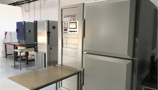
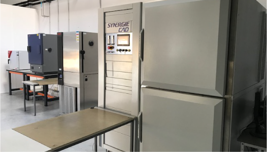
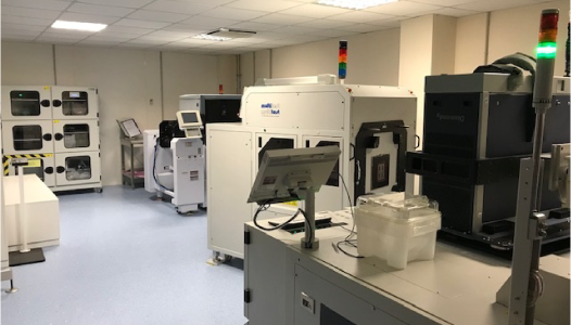
Synergie Cad can manage in-house complete Design and Manufacturing processes, coordinated by
Internal CAM teams working in full Synergy,
guaranteeing:
- Continuous Process Optimization
- Embedded Quality Improvement
- Application Performance Enhancement
- Overall Cost of Test reduction
- Flexibility in activity planning with respect to Customers Requirements
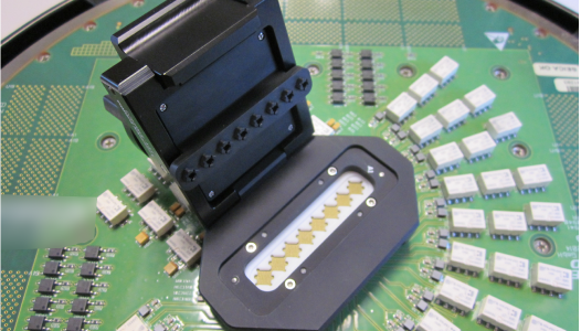
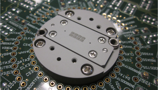
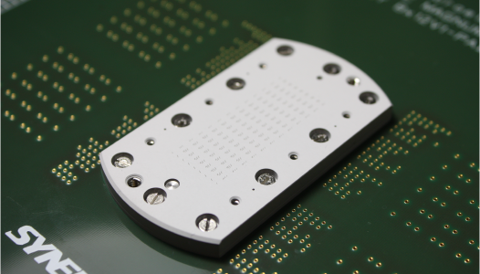
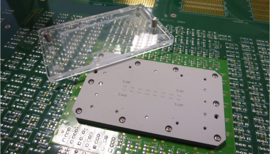
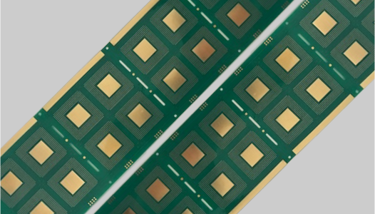
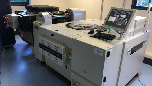
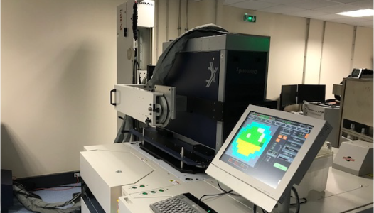
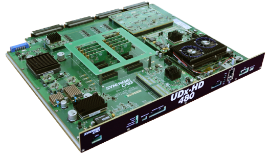
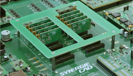
Synergie Cad capabilities are:
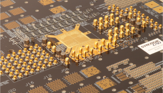
- Up to 60 multi-layers
- Thickness: up to 7.0mm
- Wide area PCB capability: 750mm x 580mm
- Planarity guaranteed through CIC Technology
- Dry Film exposure (Clean Room rated 1,000)
- Laser Direct Imaging
- Laser drilling
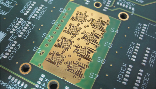
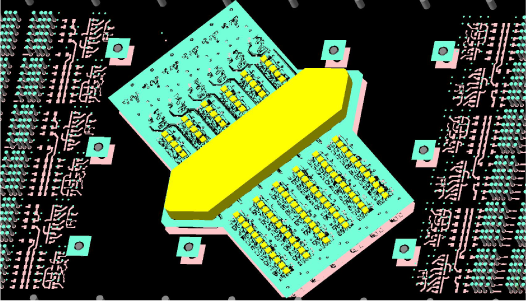
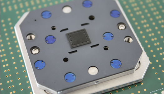
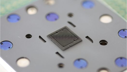
- Micro BGA boards down to 250µm pitch
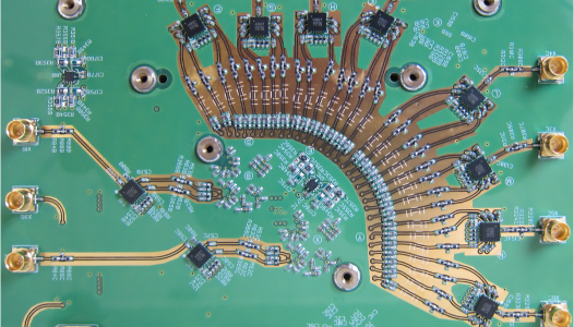
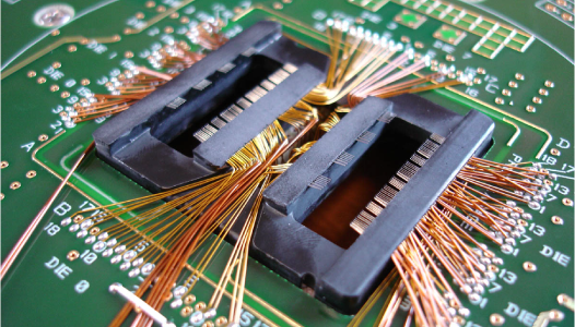
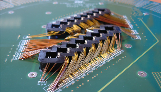
- Blind and buried vias capability
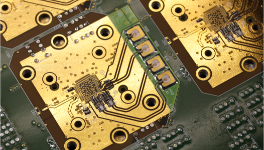
- Hole diameter 75µm
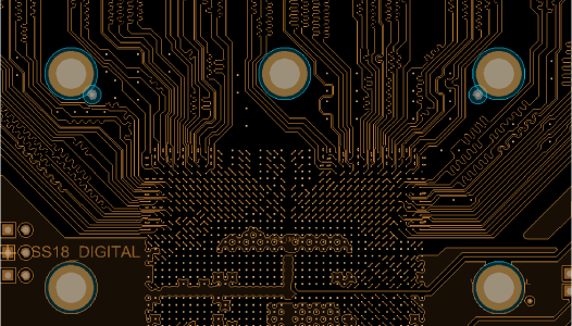
- Impedance Control
- Advanced fine pitch PCB interposers